Description
Applications:
|
|
Features:
|
|
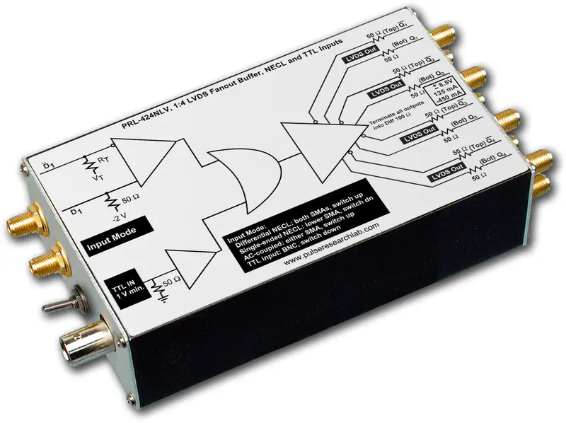
DescriptionThe PRL-424NLV is a 1:4 fanout, complementary output, LVDS line driver. It is intended for converting NECL signals, AC-coupled sine waves, or TTL signals into multiple LVDS signals for driving long lines. The PRL-424LV high speed fanout line driver facilitates testing of high speed digital communications circuits and distribution of satellite signals. The PRL-424NLV has two logically ORed input circuits:
The four pairs of complementary outputs are 50 Ω back-terminated and are designed for driving floating 100 Ω loads, normally the configuration used in LVDS input circuits. The output swing is typically 600 mV with a common mode voltage of 1.2 V. All output connectors are SMA. The PRL-424NLV is supplied with a ±8.5 V/1.8 A AC/DC adapter and housed in a 1.3 x 2.9 x 5-in. extruded aluminum enclosure. Available accessories include voltage distribution modules and brackets for mounting multiple units. (1) A related model, the PRL-424LV, has a “universal differential” input (floating 100 Ω termination) that will accept LVDS, RS-422, NECL and LVPECL, so long as the NECL and LVPECL signals are differential and have internal pull-down resistors. |
 Fig. PRL-424NLV Block Diagram
(0° C ≤ TA ≤ 35° C)*
| SYMBOL | PARAMETER | Min | Typ | Max | UNIT | Comment |
|---|---|---|---|---|---|---|
| RIN | Input Resistance | 49.5 | 50 | 50.5 | Ω | |
| VTT | D Input Termination Voltage (fixed) | -2.2 | -2.0 | -1.8 | V | |
| VT1 | D Input Termination Voltage | -1.17 | -1.30 | -1.43 | V | Switch Down |
| VT2 | D Input Termination Voltage | -2.20 | -2.00 | -1.80 | V | Switch Up |
| VIL | Input Lo Voltage | -1.95 | -1.60 | -1.48 | V | |
| VIH | Input Hi Voltage | -1.13 | -0.90 | -0.81 | V | |
| VOL | Output Low Level | 0.9 | V | |||
| VOH | Output High Level | 1.5 | V | |||
| VIL | Input Lo Voltage | -1.95 | -1.60 | -1.48 | V | |
| IDC1 | DC Input Current, +8.5 V | 130 | 140 | mA | ||
| IDC2 | DC Input Current, -8.5 V | -470 | -480 | mA | ||
| VDC | DC Input Voltage | ±7.5 | ±8.5 | ±12 | V | |
| VAC1 | AC/DC Adapter Input Voltage, 120 | 103 | 115 | 127 | V | |
| VAC1 | AC/DC Adapter Input Voltage, 220 | 206 | 220 | 254 | V | |
| tPLH | Propagation Delay to output ↑ | 2.7 | ns | |||
| tPHL | Propagation Delay to output ↓ | 2.7 | ns | |||
| tr/tf1 | Rise/Fall Times (10%-90%)1 | 500 | 650 | ps | @ 200 MHz | |
| tr/tf2 | Rise/Fall Times (10%-90%)1 | 250 | ps | @ 1.25 GHz | ||
| tSKEW | Skew between any 2 outputs | 200 | 550 | ps | ||
| fMAX1 | Max Clock Frequency, SMA Input2 | 1.25 | 1.35 | GHz | ||
| fMAX2 | Max Clock Frequency, TTL Input | 300 | MHz | |||
| Size | 1.3 x 2.9 x 5.0 | in. | ||||
| Weight | 8 | Oz | ||||
| Shipping Weight | 4 | lbs | ||||
Notes:
(1) Rise and Fall times are measured with ground-referenced 50 Ω loads.
(2) fmax is measured using the PRL-174ANT Clock Driver outputs as the driver and the PRL-425N with SMA input connectors as the receiver. The outputs of the PRL-425N are then measured. fmax for the TTL input is currently limited by the lack of TTL drivers faster than 300 MHz.
PDF Datasheet
Explore more from our collection.

Reviews
There are no reviews yet.